製品
Sumitomo Bakelite - Multiscale.Sim and Ansys software contribute to innovative materials development
Customer Interview - Sumitomo Bakelite Co., Ltd.
Multiscale.Sim and Ansys software contribute to innovative materials development
Plastic products have become an indispensable part of modern society. Sumitomo Bakelite has a long history as a comprehensive manufacturer of various plastic products used in semiconductors, electronic components, automobiles, building materials, packaging, and medical care. In 1911, the Sankyo Joint Stock Company (now Daiichi Sankyo Co., Ltd.), which was the starting point of Sumitomo Bakelite, began prototype production of phenolic resin (Bakelite). Since then, Sumitomo Bakelite has been a pioneer in plastics, providing high value-added products to the market under the motto of "creating functions rather than mere manufacturing.”
To gain deeper insight into their research and development efforts, we spoke with Mr. Takuya Hatao, Principal Researcher, and Mr. Hiroshi Nakaido, Researcher, from the Information & Telecommunication Materials Research Laboratory at Sumitomo Bakelite. This center focuses on developing materials for the rapidly evolving information and telecommunication sectors.
From left to right: Mr. Nakaido, Mr. Hatao
We aim at creating new value by combining customer needs with technologies developed through our fundamental research.
Could you tell us about your roles and responsibilities?
Hatao: We are a comprehensive manufacturer of various plastic products used in semiconductors, electronic components, automobiles, building materials, packaging, medical equipment, etc. Our business can be divided into three key areas:
- Information & Telecommunication Materials – Developing plastics used in semiconductor components, such as epoxy resin molding materials for semiconductor encapsulation.
- High-Performance Plastics – Creating materials with superior heat resistance, dimensional stability, superior mechanical properties, and wear resistance.
- Quality of Life Products – Manufacturing plastics for food packaging films, pharmaceutical packaging, and medical devices.
Its structure can be broadly divided into three divisions.
- The Fundamental Research Division that nurtures the seeds that create value for customers. They work with universities and public institutions to acquire promising technologies.
- Applied Research Department that embodies products. They have established laboratories for different product segments to enhance expertise and respond to the rapid advancement of technology.
- The Information & Telecommunication Materials Research Laboratory sits between the other two divisions and plays the role of creating value for customers by combining customer needs gathered at the Applied Research Division with promising technologies developed by the Fundamental Research Division. Most people at the research center focus on material development, while we specialize in developing reliability testing and analysis technologies to support it. CAE simulations help identify optimal material properties based on customer specifications and guide future development priorities.
The value of simulation is in predicting the future of materials: What seems "absolutely impossible" today may become a reality in a few years. Simulation is meaningful because it reveals “how to achieve what cannot be done now.
If you identify the optimal material properties, is it always possible to produce materials with those exact characteristics?
Hatao: It is not always guaranteed. Sometimes, even if the optimal material properties are known, it is impossible to make it in the same way.
However, there are cases where things that were said to be "absolutely impossible" at the time were realized a few years later and embraced by customers. In that sense, I think the significance of simulation resides in showing what you can't do right now and presenting the future direction, rather than calculating what you can do now.
What are some of the recent challenges facing the plastics industry?
Hatao: Materials and substrates, such as those used in mobile phones, have significantly accelerated product development cycles. Material design also needs to be fast, and CAE is being used to shorten the development period.
Recently, CAE simulation has become a prerequisite for customers. They have been wanting to see the results of CAE analysis to understand how much quality can be improved by using a certain material.
The ability to accurately model the effects of glass cloth made a big impact on the decision to adopt Multiscale.Sim.
What led to the adoption of Multiscale.Sim in your processes?
Hatao: This was right around the time that Multiscale.Sim™ was released. We were dealing with substrate materials, but we heard that Multiscale.Sim can model even the glass cloth inside the board, so we introduced it because it is directly related to our business. Then we purchased Multiscale.Sim together with Ansys® software.
We also use other CAE tools, but modeling glass cloth was a daunting task. However, with Multiscale.Sim, creating material microstructure models is easy. I was impressed by CYBERNET’s ability to quickly grasp customer needs and effectively commercialize them. At first, we could only work with elastic bodies, but in recent versions, viscoelasticity can also be analyzed, which is very helpful. In the case of resin products, considering viscoelasticity is indispensable.
You used our customization services too, is that correct? Could you introduce an analysis example?
Hatao: We have been using different CAE tools to perform various analyses. We have accumulated various information such as the physical properties of solder and the physical properties of resins using that tool, but there was one problem.
In general, it is better to use the transfer curing law* for solder fatigue analysis. In addition, the implicit method is suitable for efficient analysis, but the CAE tool we were using could not perform analysis using the implicit method. However, we found that Ansys could analyze it. To perform the analysis in Ansys using the material data accumulated with that tool, we asked CYBERNET to customize it.
*The transfer hardening law is a mathematical model for describing the yield behavior under a tensile-compression cyclic load. When the material yields on the tensile side, the yield stress on the compression side is lower than the initial state (Bausinger effect).
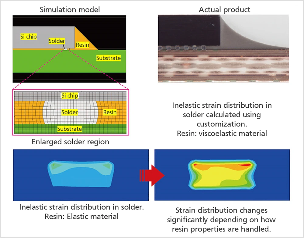
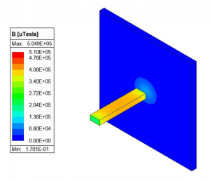
The figure shows an example of an analysis of an electronic component.
The material at the top is called chip, which has little expansion and contraction, and below that is a substrate using glass cloth. Resins are used to maintain connections between chips, circuits, and substrates, and here we analyzed the properties of resins and the effects of changes in the physical properties of substrates.
Ansys software allows you to incorporate new material models using user subroutines. In this customization, we incorporated a model in which the material properties change discontinuously at the glass transition point, i.e., at a specific temperature. How is your experience after that? If the material properties change discontinuously, does this have any effect on convergence, etc.?
Hatao: I was able to analyze it without any issues, and I am satisfied with the results. In the figure, the right side shows the case where the customized "viscoelastic" material model is used, while the left side represents the analysis performed considering it as an "elastic body" without customization. The strain distribution differs significantly between the two, demonstrating that accounting for viscoelasticity has a major impact on the analysis.
Do you consider wiring patterns and copper residual ratios in your analysis?
Hatao: The wiring pattern must be considered because it affects the analysis, but it is not feasible to model it as it is, considering the analysis time. By looking at the actual wiring pattern, we consider how it would affect the analysis and try to account for it in various ways.
It is important to clarify "what you want to see" and "why you want to see it" before you start analyzing and try to make your own predictions.
How does your company approach CAE education?
Hatao: We receive training on how to operate the CAE software through introductory seminars, etc. We learn know-how on how to model the phenomenon we want to observe and how to analyze it efficiently by contacting support teams, learning from people who actually use the software, and discussing it within our group.
What precautions do you take when utilizing CAE?
Hatao: I will try to clarify the purpose of the analysis before implementing it. What kind of results do you want to get, and how can you prove that your ideas are correct? Without that, it's easy to lose track of what you're doing along the way, or to lose sight of your original purpose by focusing on improving convergence.
Also, without understanding resin, we can't produce meaningful results for material development. That's why we make it a priority to conduct analyses alongside those who directly work with the materials.
Nakaido: The thing I'm most careful about is not to just accept the results as they come out. I always try to predict the results myself and be aware of what I want to see.
Hatao: CAE can produce results, but experimentation is necessary to properly evaluate its validity. Therefore, we try to do our own experiments as much as possible.
What are your thoughts on Ansys and Multiscale.Sim?
Nakaido: It's nice to be able to model the structure of the glass cloth in Multiscale.Sim, but in practice we are also dealing with materials with a much finer structure. For example, I think it would be nice to be able to make models with discontinuous fibers* more easily.
It seems that there are many customers who would like to be able to model short fibers easily. We are currently developing a macro that will disperse short fibers and other fillers all at once based on their content rate and orientation. In future, we would also like to be able to model even very complex microstructures, such as the stress distribution of discontinuous fiber structures inside injection molded products, with an eye toward linking with resin flow analysis tools*.
Hatao: Our resins are used in a variety of environments. The same material may exhibit completely different material properties due to different usage environments depending on the customer. Therefore, I think it would be good to be able to more easily consider the physical properties that change from time to time depending on the process.
*The original interview was conducted in 2013. Since then, many new features and enhancements have been added to Multiscale.Sim. The latest version offers robust analysis capabilities for both short fiber and discontinuous fiber-reinforced composites. It also includes templates for modeling more complex microstructures, including those with voids. Additionally, Multiscale.Sim now supports coupling with popular resin flow analysis tools such as Moldex3D®, Moldflow®, and PlanetsX™ (the latter is available in Japanese UI only). For more information, please refer to the release notes.
We expect CAE to visualize what cannot be seen through experiments. If we can analyze phenomena at the micro or molecular level, CAE can surpass the value of expensive experimental equipment.
Looking ahead, what advancements do you hope to see in CAE?
Nakaido: I would like to explore the use of high-performance computing. In the past, CAE was limited by hardware specifications, but now, most problems can be solved. Until now, we have simplified less critical parts as much as possible during analysis. If more detailed models are used for analyses eliminating such simplifications, we may uncover new possibilities.
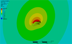
Hatao: At the same time, of course, we also want to dive into the finer details. That’s really where CAE shines—making the invisible visible. Take the solder cross-section I showed earlier, for example. If you use specialized equipment, you can get a detailed and clear image, but there’s always a limit to how much you can see.
With CAE, if we can analyze things down to the micro or even molecular level, understand the structure in those regions, and see what kind of effects they have, then CAE could become an even more valuable tool—maybe even more useful than expensive experimental equipment.
Ansys' parallel computing capabilities have also been greatly enhanced. In addition to glass cloth, semiconductor packages have inhomogeneous parts such as porous materials everywhere. I think it is a part that cannot be fully analyzed by experiments, so I think it would be a great advantage if it could be analyzed with Multiscale.Sim.
Do you have any requests for us?
Hatao: In addition to providing software, I think it would be good if you could also provide information on technological trends, such as what products are currently gaining attention, what products are likely to grow in the future, and problems that may arise as a result. CYBERNET has a large number of customers, so it may be easy to gather information.
Thank you. We aim to provide as much information as possible based on customer references.
This interview was first published in Japanese in "Manufacturing with CAE Vol.19 2013"
関連情報
関連する解析事例
MORE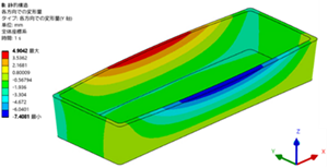
関連する資料ダウンロード
MORE-
【カタログ】3Dデザインソリューション
-
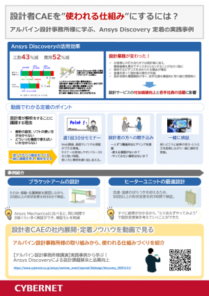
設計者CAEを”使われる仕組み”にするには?
アルパイン設計事務所様に学ぶ、Ansys Discovery 定着の実践事例
-
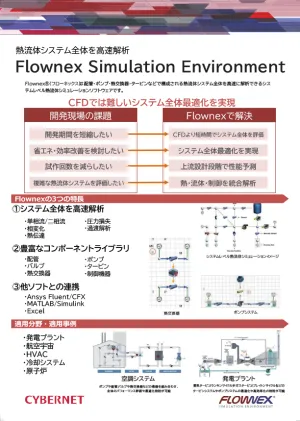
熱流体システム全体を高速解析ーFlownex Simulation Environmentー
-
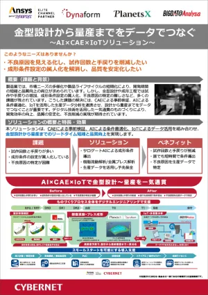
金型設計から量産までをIoT生産データでつなぐ一気通貫のものづくり
-
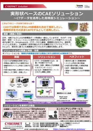
実形状ベースのCAEソリューション
~CTデータを活用した高精度シミュレーション~
-
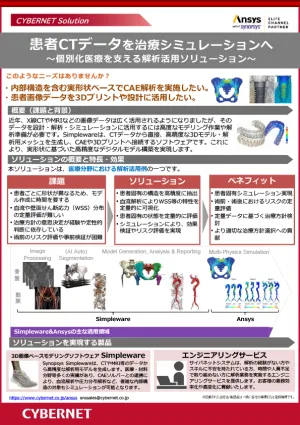
患者CTデータを治療シミュレーションへ
~個別化医療を支える解析活用ソリューション~
-
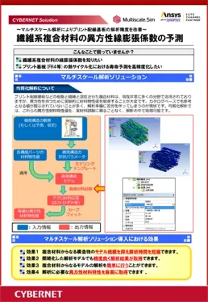
繊維系複合材料の異方性線膨張係数の予測
~マルチスケール解析によりプリント配線基板の解析精度を改善~
-
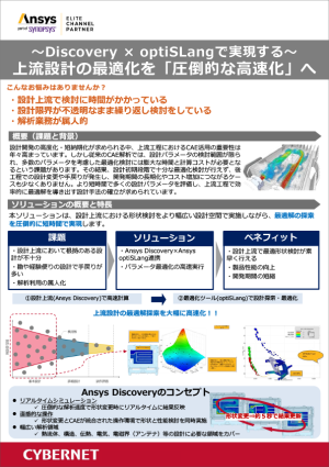
短時間で設計パラメータを評価。上流設計の最適化を「圧倒的な高速化」へ
設計上流における形状検討をより幅広い設計空間で実施